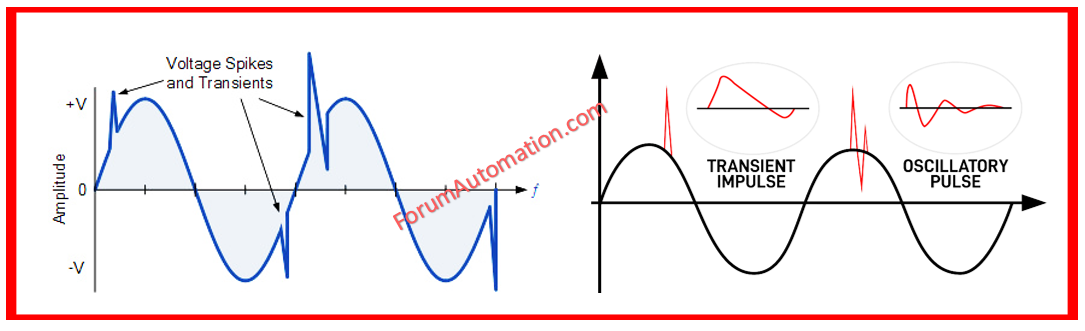
The smoke curling upward from a newly minted prototype is an engineer’s distinct heartbreak. On the bench, everything looked pristine. The firmware booted cleanly, the microcontrollers negotiated packets at lightning speed, and the power delivery network hummed at exact ripple tolerances. Yet, the moment a heavy inductive motor kicked on three benches down, or a distant summer storm induced a transient wave across the main power lines, the board went completely silent. The onboard digital brain was instantly vaporized by a phantom surge that slipped past the primary fuse.
Most post-mortem analyses of fried electronics point the finger at a component failure. Engineers swap out a dead microcontroller, drop in a beefier voltage regulator, and pray for a better outcome during the next compliance run. Almost invariably, the replacement board suffers the exact same fate. The underlying flaw is rarely a weak individual part. Instead, it is an absence of coordinated orchestration across the entire circuit board topography.
Protecting modern, delicate silicon from the violent reality of the outside world requires an architectural shift. A single line of defense is mathematically incapable of surviving high-energy lightning strikes while simultaneously clamping microvolt-level static spikes. Solving this engineering paradox demands a multi-stage approach. By deploying Gas Discharge Tubes (GDTs), Metal Oxide Varistors (MOVs), and Transient Voltage Suppressors (TVS diodes) in a meticulously timed hierarchy, designers can build robust, unyielding circuit boards capable of shunting thousands of volts safely into the chassis ground.
The Triad of Transient Suppression: Understanding GDT, MOV, and TVS Core Physics
Every suppression technology on the market operates under a fundamental compromise between speed, energy handling, and clamping precision. No single device can do it all. To understand why a layered defense strategy is mandatory, we must first break down the physical characteristics of the three pillars of circuit protection: Gas Discharge Tubes, Metal Oxide Varistors, and Transient Voltage Suppressors.
Gas Discharge Tubes act as the heavyweight champions of energy absorption. Inside a hermetically sealed ceramic or glass envelope, two or three electrodes sit across a rare-gas mixture such as argon or neon. Under normal operating voltages, the gas acts as an exceptional insulator, exhibiting gigohms of resistance with negligible leakage current. However, when an overvoltage transient exceeds the DC spark-over voltage, the gas ionizes and transitions into a plasma arc. This crowbar behavior drops the voltage across the device to a mere 10 to 30 volts while shunting kiloamps of surge current. The catch? Physics takes time. GDTs suffer from a relatively slow response time, often requiring several hundred nanoseconds or even a microsecond to ignite. If a fast, sharp transient hits the board, destructive energy will pass straight through the terminals before the gas breaks down.
Metal Oxide Varistors sit in the middle of the hierarchy, offering a balance of high energy handling and faster clamping than a GDT. Constructed from a sintered matrix of zinc oxide grains interspersed with other metal oxides like bismuth or manganese, an MOV behaves like a collection of back-to-back Zener diodes. When a voltage spike crosses its threshold, the intergranular boundaries experience a rapid non-linear drop in resistance, conducting current away from sensitive nodes. MOVs can absorb thousands of joules, making them ideal for AC mains inputs and heavy industrial lines. However, they carry a distinct operational penalty: wear and tear. Every transient an MOV absorbs degrades its internal structure, progressively lowering its clamping voltage and increasing leakage current until it eventually fails via thermal runaway or short circuit.
Transient Voltage Suppressor diodes operate at the opposite end of the spectrum. Built using specialized silicon p-n junction architecture, TVS diodes offer blindingly fast response times, clamping overvoltage events in picoseconds. Their clamping voltage is exceptionally tight, protecting delicate microprocessors, interface transceivers, and high-speed data lines from catastrophic latch-up. Yet, silicon lacks the massive physical mass required to survive high-energy strikes. Direct exposure to a lightning surge will vaporize a standard TVS diode instantly. They are designed to clip the razor-sharp residual edges of a transient that has already been battered down by downstream heavyweights.
The Mechanics of Staged Coordination and Energy Hand-Off
Deploying a GDT, an MOV, and a TVS diode on the same printed circuit board without a coordination strategy is a recipe for disaster. If these components are wired in parallel directly across a node without impedance between them, the fastest device will take the brunt of the strike, or the components will fight each other based on their respective turn-on thresholds. True protection relies on a relay race of physics, where each component passes the baton of suppression to the next in line.
The secret to a successful multi-stage topology lies in the strategic placement of series decoupling elements. A series impedance—typically a carefully calculated trace inductance, a high-power wirewound resistor, or a ferrite bead—must be inserted between the primary heavy-duty stage and the secondary fine-clamping stage. When a massive transient wave strikes the board entrance, the GDT or primary MOV fires first, absorbing the lion’s share of the energy.
However, because the GDT or MOV has a high clamping voltage and finite response time, a fast, jagged voltage spike bleeds past into the interior of the circuit. The series inductor acts as a traffic cop for this residual energy. By choking the rate of current change ($di/dt$), the inductor delays the arrival of the wavefront at the secondary stage, buying precious nanoseconds for the downstream TVS diode to wake up and cleanly clip the remaining voltage to a safe level. Without this series decoupling element, the fast transient outruns the slow components, destroying downstream silicon before the heavy hitters even register the fault.
Step-by-Step Implementation of a Layered PCB Protection Circuit
Designing an effective multi-stage protection circuit requires a methodical approach that accounts for trace geometry, component spacing, and electrical parameters. Skipping even a single layout rule can completely invalidate the theoretical protection limits of your chosen parts.
- Step 1 (Define the Threat Environment and Standards): Review the operational environment and applicable compliance standards, such as IEC 61000-4-5 for surge immunity or IEC 61000-4-2 for electrostatic discharge. Determine the maximum continuous operating voltage (MCOV) of your circuit and establish peak surge current expectations, such as a 1.2/50µs combined wave generator profile.
- Step 2 (Select the Primary Defense Component): Choose a high-energy GDT or high-capacity MOV to sit directly at the board entry connector. For AC mains or exposed industrial wiring, a 3-electrode GDT paired with a high-surge MOV offers robust common-mode and differential-mode defense. Ensure the voltage rating sits safely above your maximum working voltage plus tolerance margins.
- Step 3 (Integrate the Series Decoupling Impedance): Place a low-resistance, high-power-rated inductor or coordinated trace inductance immediately downstream of your primary stage. This component must be physically capable of handling normal operating currents without saturating while providing enough reactive impedance to slow down transient rise times for downstream stages.
- Step 4 (Position the Secondary Fine-Clamping TVS Diodes): Locate your TVS diodes as physically close as possible to the sensitive integrated circuits, microcontrollers, or communication ports they are guarding. Ensure the TVS standoff voltage is higher than the normal signal swing while keeping its clamping voltage well below the absolute maximum rating of the protected IC.
- Step 5 (Optimize Ground Return Planes and Routing): Route all transient suppression grounds through a low-inductance, low-impedance path back to the primary earth or chassis ground connection. Avoid narrow traces, sharp 90-degree corners, and long via chains that add parasitic inductance and cause dangerous voltage bounces during a high-current discharge event.
Avoiding Critical Layout Pitfalls and Design Traps
Even with top-tier components, poor printed circuit board layout practices can render a sophisticated protection scheme entirely useless. Transient voltages operate under brutal high-frequency laws where every millimeter of copper trace introduces parasitic inductance capable of generating hundreds of unwanted volts during a high-$di/dt$ strike.
- Pitfall 1 (Long Stub Traces on Protection Components): Placing protection components off to the side on long stub traces creates an inductive voltage divider. During a surge, the voltage drop across the stray inductance of the stub trace can easily exceed the clamping voltage of the device, routing the destructive surge directly into the protected IC instead of the suppressor.
Workaround: Route high-energy traces directly through the pads of the protection components (kelvin or daisy-chain connection style) rather than branching off via stubs. - Pitfall 2 (Inadequate Clearance and Creepage Distances): Under high-voltage surges, air can ionize, causing an arc-over between unprotected traces and suppression components, bypassing the protection network entirely.
Workaround: Maintain strict IPC-2221 or IEC 60664 clearance standards on the input side of the board. Implement physical milling slots or air gaps in the PCB substrate beneath the GDT to prevent carbon tracking after repeated firing events. - Pitfall 3 (Uncoordinated Component Voltages): Selecting a TVS diode whose clamping voltage is lower than the firing threshold of the upstream MOV or GDT can result in the TVS absorbing energy it was never designed to handle, leading to an instant thermal blowout.
Workaround: Calculate the dynamic resistance and clamping hierarchy meticulously. Ensure the upstream device drops voltage aggressively before the downstream device reaches its peak power dissipation rating. - Pitfall 4 (Polluting Quiet Ground Planes with Surge Currents): Dumping high-energy transient currents directly into the sensitive analog or digital ground plane of a mixed-signal board causes massive ground bounce, corrupting data and resetting processors.
Workaround: Establish a dedicated, isolated surge ground zone at the input connector where all primary GDT and MOV returns terminate, tying this zone to the chassis earth via a high-voltage capacitor or a heavily reinforced star-ground connection. - Pitfall 5 (Neglecting Thermal Degradation and Failure Modes): Designing MOVs without accounting for their end-of-life failure mode, which frequently involves short-circuiting and extreme heat generation.
Workaround: Always pair MOVs with thermal fuses or disconnects (TCOs) physically coupled to the varistor body to safely open the circuit before a catastrophic thermal runaway or board fire occurs.
The Broader Ecosystem: Economic Value, Long-Term Reliability, and Modern Trends
Integrating a rigorous layered defense strategy changes the economic calculus of electronic product development. While adding GDTs, MOVs, TVS arrays, and the associated PCB real estate incurs a minor upfront BOM (Bill of Materials) cost, it pays massive dividends over the lifecycle of the hardware. In industrial automation, agricultural machinery, and outdoor IoT deployments, a single field service truck roll to replace a lightning-fried circuit board can easily eclipse the total component cost of an entire production run’s surge protection network. Designing for survivability transforms hardware from a fragile liability into a rugged, trusted asset.
Looking across the engineering landscape, the demands placed on circuit protection are intensifying. As communication protocols run at higher frequencies, the parasitic capacitance introduced by high-energy protection components threatens signal integrity. Modern TVS manufacturers have responded by developing ultra-low capacitance arrays (often under 0.5pF) capable of protecting multi-gigabit Ethernet, USB4, and automotive Ethernet lines without distorting eye diagrams. Simultaneously, advancements in zinc-oxide formulation have yielded high-surge MOVs with dramatically lower degradation profiles, extending operational lifespans in harsh, lightning-prone environments.
Furthermore, compliance testing has grown increasingly stringent. Regulatory frameworks around the globe now demand higher immunity margins against complex, multi-pulse transient threats. Engineers can no longer rely on rule-of-thumb approximations or generic reference schematics. Modern design workflows require rigorous SPICE simulation of transient waveforms against coupled parasitic circuit models before a single gerber file is sent to the fabrication house.
Actionable Recommendations for Bulletproof PCB Design
To synthesize these principles into an actionable workflow for your next hardware project, anchor your design decisions in structural discipline and empirical verification:
- Enforce the Input-First Rule: Always position your primary heavy-duty protection (GDT/MOV) immediately where the external cable or connector interfaces with the board edge, before any filtering, fusing, or power conversion stages.
- Embrace Multi-Stage Hierarchy: Never rely on a single component type. Pair a slow, high-energy crowbar device with a fast, precision-clamping silicon device, separated by verified series impedance.
- Minimize Loop Areas: Keep all trace lengths connecting protection components to absolute minimums. Reduce loop areas to prevent electromagnetic induction from coupling transient energy into nearby traces.
- Validate with IEC 61000-4-5 Simulation and Testing: Do not guess your protection limits. Run transient circuit simulations incorporating trace parasitics, and validate physical prototypes using accredited surge generator test benches to ensure your board survives real-world abuse.
The invisible world of electrical transients is relentless, chaotic, and unforgiving. Every time a relay clicks, a motor brakes, or a storm cloud discharges static electricity into the atmosphere, your circuit board stands in the path of destruction. Treating circuit protection as an afterthought or a last-minute compliance checkbox is a gamble that engineering teams inevitably lose.
By embracing a layered defense philosophy—where Gas Discharge Tubes absorb the brunt of massive energy, Metal Oxide Varistors smooth the intermediate wave, and TVS diodes stand guard over delicate silicon—you establish an impenetrable hierarchy. Success in modern PCB design is not merely about making a circuit function in the pristine environment of a laboratory. It is about engineering resilience, ensuring that your hardware stands strong against the unpredictable electrical storms of the real world.